

TDA2030 - Datasheet Catalog
TDA2030 - Datasheet Catalog
TDA2030 - Datasheet Catalog

Create successful ePaper yourself
Turn your PDF publications into a flip-book with our unique Google optimized e-Paper software.
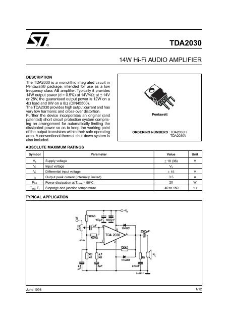
® <strong>TDA2030</strong><br />
14W Hi-Fi AUDIO AMPLIFIER<br />
DESCRIPTION<br />
The <strong>TDA2030</strong> is a monolithic integrated circuit in<br />
Pentawatt® package, intended for use as a low<br />
frequency class AB amplifier. Typically it provides<br />
14W output power (d = 0.5%) at 14V/4Ω; at ± 14V<br />
or 28V, the guaranteed output power is 12W on a<br />
4Ω load and 8W on a 8Ω (DIN45500).<br />
The <strong>TDA2030</strong> provides high output current and has<br />
very low harmonic and cross-over distortion.<br />
Further the device incorporates an original (and<br />
patented) short circuit protection system comprising<br />
an arrangement for automatically limiting the<br />
dissipated power so as to keep the working point<br />
of the output transistors within their safe operating<br />
area. A conventional thermal shut-down system is<br />
also included.<br />
Pentawatt<br />
ORDERING NUMBERS : <strong>TDA2030</strong>H<br />
<strong>TDA2030</strong>V<br />
ABSOLUTE MAXIMUM RATINGS<br />
Symbol Parameter Value Unit<br />
V s Supply voltage ± 18 (36) V<br />
V i Input voltage V s<br />
V i Differential input voltage ± 15 V<br />
I o Output peak current (internally limited) 3.5 A<br />
P tot Power dissipation at T case = 90°C 20 W<br />
T stg , T j Stoprage and junction temperature -40 to 150 °C<br />
TYPICAL APPLICATION<br />
June 1998<br />
1/12
<strong>TDA2030</strong><br />
PIN CONNECTION (top view)<br />
+V S<br />
OUTPUT<br />
-V S<br />
INVERTING INPUT<br />
NON INVERTING INPUT<br />
TEST CIRCUIT<br />
2/12
<strong>TDA2030</strong><br />
THERMAL DATA<br />
Symbol Parameter Value Unit<br />
R th j-case Thermal resistance junction-case max 3 °C/W<br />
ELECTRICAL CHARACTERISTICS (Refer to the test circuit, Vs = ± 14V , Tamb = 25°C unless otherwise<br />
specified) for single Supply refer to fig. 15 Vs = 28V<br />
Symbol Parameter Test conditions Min. Typ. Max. Unit<br />
V s Supply voltage<br />
± 6<br />
12<br />
± 18<br />
36<br />
V<br />
I d<br />
Quiescent drain current<br />
40 60 mA<br />
I b Input bias current 0.2 2 µA<br />
V os Input offset voltage<br />
V s = ± 18V (Vs = 36V)<br />
± 2 ± 20 mV<br />
I os Input offset current ± 20 ± 200 nA<br />
P o Output power d = 0.5% G v = 30 dB<br />
f = 40 to 15,000 Hz<br />
R L = 4Ω<br />
R L = 8Ω<br />
12<br />
8<br />
14<br />
9<br />
W<br />
W<br />
d = 10%<br />
f = 1 KHz<br />
R L = 4Ω<br />
R L = 8Ω<br />
G v = 30 dB<br />
18<br />
11<br />
W<br />
W<br />
d Distortion P o = 0.1 to 12W<br />
R L = 4Ω G v = 30 dB<br />
f = 40 to 15,000 Hz 0.2 0.5 %<br />
P o = 0.1 to 8W<br />
R L = 8Ω G v = 30 dB<br />
f = 40 to 15,000 Hz 0.1 0.5 %<br />
B<br />
Power Bandwidth<br />
(-3 dB)<br />
G v = 30 dB<br />
P o = 12W<br />
R L = 4Ω<br />
10 to 140,000 Hz<br />
R i Input resistance (pin 1) 0.5 5 MΩ<br />
G v Voltage gain (open loop) 90 dB<br />
G v Voltage gain (closed loop) f = 1 kHz 29.5 30 30.5 dB<br />
e N Input noise voltage B = 22 Hz to 22 KHz 3 10 µV<br />
i N Input noise current 80 200 pA<br />
SVR Supply voltage rejection R L = 4Ω G v = 30 dB<br />
R g = 22 kΩ<br />
V ripple = 0.5 V eff<br />
f ripple = 100 Hz<br />
40 50 dB<br />
I d Drain current P o = 14W<br />
P o = W<br />
R L = 4Ω<br />
R L = 8Ω<br />
900<br />
500<br />
mA<br />
mA<br />
3/12
<strong>TDA2030</strong><br />
Figure 1. Output power vs.<br />
supply voltage<br />
Figure 2. Output power vs.<br />
supply voltage<br />
Figure 3. Distortion vs.<br />
output power<br />
Figure 4. Distortion vs.<br />
output power<br />
Figure 5. Distortion vs.<br />
output power<br />
Figure 6. Distortion vs.<br />
frequency<br />
Figure 7. Distortion vs.<br />
frequency<br />
Figure 8. Frequency response<br />
with different values<br />
of the rolloff capacitor C8<br />
(see fig. 13)<br />
Figure 9. Quiescent current<br />
vs. supply voltage<br />
4/12
<strong>TDA2030</strong><br />
Figure 10. Supply voltage<br />
rejection vs. voltage gain<br />
Figure 11. Power dissipation<br />
and efficiency vs. output<br />
power<br />
Figure 12. Maximum power<br />
dissipation vs. supply voltage<br />
(sine wave operation)<br />
APPLICATION INFORMATION<br />
Figure 13. Typical amplifier<br />
with split power supply<br />
Figure 14. P.C. board and component layout for<br />
the circuit of fig. 13 (1 : 1 scale)<br />
5/12
<strong>TDA2030</strong><br />
APPLICATION INFORMATION (continued)<br />
Figure 15. Typical amplifier<br />
with single power supply<br />
Figure 16. P.C. board and component layout for<br />
the circuit of fig. 15 (1 : 1 scale)<br />
Figure 17. Bridge amplifier configuration with split power supply (Po = 28W, Vs = ±14V)<br />
6/12
<strong>TDA2030</strong><br />
PRACTICAL CONSIDERATIONS<br />
Printed circuit board<br />
The layout shown in Fig. 16 should be adopted by<br />
the designers. If different layouts are used, the<br />
ground points of input 1 and input 2 must be well<br />
decoupled from the ground return of the output in<br />
which a high current flows.<br />
Assembly suggestion<br />
No electrical isolation is needed between the<br />
package and the heatsink with single supply voltage<br />
configuration.<br />
Application suggestions<br />
The recommended values of the components are<br />
those shown on application circuit of fig. 13.<br />
Different values can be used. The following table<br />
can help the designer.<br />
Component<br />
Recomm.<br />
value<br />
Purpose<br />
Larger than<br />
recommended value<br />
Smaller than<br />
recommended value<br />
R1 22 kΩ Closed loop gain<br />
setting<br />
Increase of gain Decrease of gain (*)<br />
R2 680 Ω Closed loop gain<br />
setting<br />
R3 22 kΩ Non inverting input<br />
biasing<br />
Decrease of gain (*)<br />
Increase of input<br />
impedance<br />
Increase of gain<br />
Decrease of input<br />
impedance<br />
R4 1 Ω Frequency stability Danger of osccilat. at<br />
high frequencies<br />
with induct. loads<br />
R5 ≅ 3 R2 Upper frequency<br />
cutoff<br />
C1 1 µF Input DC<br />
decoupling<br />
C2 22 µF Inverting DC<br />
decoupling<br />
C3, C4 0.1 µF Supply voltage<br />
bypass<br />
C5, C6 100 µF Supply voltage<br />
bypass<br />
Poor high frequencies<br />
attenuation<br />
Danger of<br />
oscillation<br />
Increase of low<br />
frequencies cutoff<br />
Increase of low<br />
frequencies cutoff<br />
Danger of<br />
oscillation<br />
Danger of<br />
oscillation<br />
C7 0.22 µF Frequency stability Danger of oscillation<br />
C8<br />
≅<br />
1<br />
2π B R1<br />
Upper frequency<br />
cutoff<br />
Smaller bandwidth<br />
Larger bandwidth<br />
D1, D2 1N4001 To protect the device against output voltage spikes<br />
(*) Closed loop gain must be higher than 24dB<br />
7/12
<strong>TDA2030</strong><br />
SINGLE SUPPLY APPLICATION<br />
Component<br />
Recomm.<br />
value<br />
Purpose<br />
Larger than<br />
recommended value<br />
Smaller than<br />
recommended value<br />
R1 150 kΩ Closed loop gain<br />
setting<br />
Increase of gain Decrease of gain (*)<br />
R2 4.7 kΩ Closed loop gain<br />
setting<br />
R3 100 kΩ Non inverting input<br />
biasing<br />
Decrease of gain (*)<br />
Increase of input<br />
impedance<br />
Increase of gain<br />
Decrease of input<br />
impedance<br />
R4 1 Ω Frequency stability Danger of osccilat. at<br />
high frequencies<br />
with induct. loads<br />
R A /R B 100 kΩ Non inverting input Biasing Power Consumption<br />
C1 1 µF Input DC<br />
decoupling<br />
C2 22 µF Inverting DC<br />
decoupling<br />
C3 0.1 µF Supply voltage<br />
bypass<br />
C5 100 µF Supply voltage<br />
bypass<br />
Increase of low<br />
frequencies cutoff<br />
Increase of low<br />
frequencies cutoff<br />
Danger of<br />
oscillation<br />
Danger of<br />
oscillation<br />
C7 0.22 µF Frequency stability Danger of oscillation<br />
C8<br />
≅<br />
1<br />
2π B R1<br />
Upper frequency<br />
cutoff<br />
Smaller bandwidth<br />
Larger bandwidth<br />
D1, D2 1N4001 To protect the device against output voltage spikes<br />
(*) Closed loop gain must be higher than 24dB<br />
8/12
<strong>TDA2030</strong><br />
SHORT CIRCUIT PROTECTION<br />
The <strong>TDA2030</strong> has an original circuit which limits the<br />
current of the output transistors. Fig. 18 shows that<br />
the maximum output current is a function of the<br />
collector emitter voltage; hence the output transistors<br />
work within their safe operating area (Fig. 2).<br />
This function can therefore be considered as being<br />
peak power limiting rather than simple current limiting.<br />
It reduces the possibility that the device gets damaged<br />
during an accidental short circuit from AC<br />
output to ground.<br />
Figure 18. Maximum<br />
output current vs.<br />
voltage [VCEsat] across<br />
each output transistor<br />
Figure 19. Safe operating area and<br />
collector characteristics of the<br />
protected power transistor<br />
THERMAL SHUT-DOWN<br />
The presence of a thermal limiting circuit offers the<br />
following advantages:<br />
1. An overload on the output (even if it is permanent),<br />
or an above limit ambient temperature can<br />
be easily supported since the Tj cannot be<br />
higher than 150°C.<br />
2. The heatsink can have a smaller factor of safety<br />
compared with that of a conventional circuit.<br />
There is no possibility of device damage due to<br />
high junction temperature. If for any reason, the<br />
junction temperature increases up to 150°C, the<br />
thermal shut-down simply reduces the power<br />
dissipation at the current consumption.<br />
The maximum allowable power dissipation depends<br />
upon the size of the external heatsink (i.e. its<br />
thermal resistance); fig. 22 shows this dissipable<br />
power as a function of ambient temperature for<br />
different thermal resistance.<br />
9/12
<strong>TDA2030</strong><br />
Figure 20. Output power and<br />
drain current vs. case<br />
temperature (RL = 4Ω)<br />
Figure 21. Output power and<br />
drain current vs. case<br />
temperature (RL = 8Ω)<br />
Figure 22. Maximum<br />
allowable power dissipation<br />
vs. ambient temperature<br />
Figure 23. Example of heat-sink<br />
Dimension : suggestion.<br />
The following table shows the length that<br />
the heatsink in fig. 23 must have for several<br />
values of Ptot and Rth.<br />
Ptot (W) 12 8 6<br />
Length of heatsink<br />
(mm)<br />
60 40 30<br />
Rth of heatsink<br />
(° C/W)<br />
4.2 6.2 8.3<br />
10/12
<strong>TDA2030</strong><br />
PENTAWATT PACKAGE MECHANICAL DATA<br />
DIM.<br />
mm<br />
inch<br />
MIN. TYP. MAX. MIN. TYP. MAX.<br />
A 4.8 0.189<br />
C 1.37 0.054<br />
D 2.4 2.8 0.094 0.110<br />
D1 1.2 1.35 0.047 0.053<br />
E 0.35 0.55 0.014 0.022<br />
E1 0.76 1.19 0.030 0.047<br />
F 0.8 1.05 0.031 0.041<br />
F1 1 1.4 0.039 0.055<br />
G 3.2 3.4 3.6 0.126 0.134 0.142<br />
G1 6.6 6.8 7 0.260 0.268 0.276<br />
H2 10.4 0.409<br />
H3 10.05 10.4 0.396 0.409<br />
L 17.55 17.85 18.15 0.691 0.703 0.715<br />
L1 15.55 15.75 15.95 0.612 0.620 0.628<br />
L2 21.2 21.4 21.6 0.831 0.843 0.850<br />
L3 22.3 22.5 22.7 0.878 0.886 0.894<br />
L4 1.29 0.051<br />
L5 2.6 3 0.102 0.118<br />
L6 15.1 15.8 0.594 0.622<br />
L7 6 6.6 0.236 0.260<br />
L9 0.2 0.008<br />
M 4.23 4.5 4.75 0.167 0.177 0.187<br />
M1 3.75 4 4.25 0.148 0.157 0.167<br />
V4<br />
40° (typ.)<br />
Dia 3.65 3.85 0.144 0.152<br />
L<br />
V<br />
L1<br />
L8<br />
V1<br />
V<br />
R<br />
V3<br />
R<br />
E<br />
M1<br />
V<br />
V<br />
A<br />
B<br />
C<br />
L5<br />
D1<br />
L2<br />
L3<br />
D<br />
R<br />
V4<br />
M<br />
H2<br />
V4<br />
E<br />
F<br />
E1<br />
H3<br />
H1<br />
G<br />
G1<br />
Dia.<br />
L7<br />
L6<br />
F1<br />
F<br />
H2<br />
RESIN BETWEEN<br />
LEADS<br />
L9<br />
V4<br />
11/12
<strong>TDA2030</strong><br />
Information furnished is believed to be accurate and reliable. However, STMicroelectronics assumes no responsibility for the consequences of<br />
use of such information nor for any infringement of patents or other rights of third parties which may result from its use. No license is granted<br />
by implication or otherwise under any patent or patent rights of STMicroelectronics. Specification mentioned in this publication are subject to<br />
change without notice. This publication supersedes and replaces all information previously supplied. STMicroelectronics products are not<br />
authorized for use as critical components in life support devices or systems without express written approval of STMicroelectronics.<br />
The ST logo is a registered trademark of STMicroelectronics<br />
© 1998 STMicroelectronics – Printed in Italy – All Rights Reserved<br />
STMicroelectronics GROUP OF COMPANIES<br />
Australia - Brazil - Canada - China - France - Germany - Italy - Japan - Korea - Malaysia - Malta - Mexico - Morocco - The Netherlands -<br />
Singapore - Spain - Sweden - Switzerland - Taiwan - Thailand - United Kingdom - U.S.A.<br />
12/12
This datasheet has been download from:<br />
www.datasheetcatalog.com<br />
<strong>Datasheet</strong>s for electronics components.


