

TDA2052 - Datasheet Catalog
TDA2052 - Datasheet Catalog
TDA2052 - Datasheet Catalog

Create successful ePaper yourself
Turn your PDF publications into a flip-book with our unique Google optimized e-Paper software.
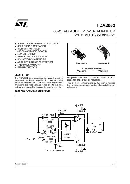
®<br />
<strong>TDA2052</strong><br />
60W Hi-Fi AUDIO POWER AMPLIFIER<br />
WITH MUTE / STAND-BY<br />
SUPPLY VOLTAGE RANGE UP TO ±25V<br />
SPLIT SUPPLY OPERATION<br />
HIGH OUTPUT POWER<br />
(UP TO 60W MUSIC POWER)<br />
LOW DISTORTION<br />
MUTE/STAND-BY FUNCTION<br />
NO SWITCH ON/OFF NOISE<br />
AC SHORT CIRCUIT PROTECTION<br />
THERMAL SHUTDOWN<br />
ESD PROTECTION<br />
TEST AND APPLICATION CIRCUIT<br />
Heptawatt V<br />
Heptawatt H<br />
ORDERING NUMBERS:<br />
<strong>TDA2052</strong>V<br />
<strong>TDA2052</strong>H<br />
DESCRIPTION<br />
The <strong>TDA2052</strong> is a monolithic integrated circuit in<br />
Heptawatt package, intended for use as audio<br />
class AB amplifier in TV or Hi-Fi field application.<br />
Thanks to the wide voltage range and to the high<br />
out current capability it’s able to supply the highest<br />
power into both 4Ω and 8Ω loads even in<br />
presence of poor supply regulation.<br />
The built in Muting/Stand-by function simplifies<br />
the remote operations avoiding also switching onoff<br />
noises.<br />
January 2003<br />
This is advanced information on a new product now in development or undergoing evaluation. Details are subject to change without notice.<br />
1/14
<strong>TDA2052</strong><br />
ABSOLUTE MAXIMUM RATINGS<br />
Symbol Parameter Value Unit<br />
V S DC Supply Voltage ±25 V<br />
I O Output Peak Current (internally limited) 6 A<br />
P tot Power Dissipation T case = 70°C 30 W<br />
T op Operating Temperature Range 0 to +70 °C<br />
T stg , T j Storage and Junction Temperature -40 to +150 °C<br />
PIN CONNECTION (Top view)<br />
7 NON INVERTING INPUT(PLAY)<br />
6<br />
INVERTING INPUT<br />
5<br />
NON INVERTING INPUT(MUTE)<br />
4<br />
-V S<br />
3<br />
STAND-BY/MUTE<br />
2<br />
+V S<br />
1<br />
OUTPUT<br />
tab connected to pin 4<br />
D95AU326<br />
BLOCK DIAGRAM<br />
2/14
<strong>TDA2052</strong><br />
THERMAL DATA<br />
Symbol Description Value Unit<br />
R th j-case Thermal Resistance Junction-case Max 2.5 °C/W<br />
ELECTRICAL CHARACTERISTICS (Refer to the test circuit, GV = 32dB; VS + 18V; f = 1KHz; Tamb =<br />
25°C, unless otherwise specified.)<br />
Symbol Parameter Test Condition Min. Typ. Max. Unit<br />
V S Supply Range +6 +25 V<br />
I q Total Quiescent Current V S = +22V 20 40 70 mA<br />
I b Input Bias Current +0.5 µA<br />
V OS Input Offset Voltage +15 mV<br />
I OS Input Offset Current +200 nA<br />
P O<br />
Music Output Power<br />
IEC268-3 Rules (*)<br />
P O Output Power (continuous RMS) d = 10%<br />
RL = 4Ω<br />
R L = 8Ω<br />
V S = +22V, R L = 8Ω<br />
d = 1%<br />
R L = 4Ω<br />
R L = 8Ω<br />
V S = +22V, R L = 8Ω<br />
d Total Harmonic Distortion R L = 4Ω<br />
P O = 0.1 to 20W;<br />
f = 100Hz to 15KHz<br />
V S = + 22.5, R L = 4Ω,<br />
d = 10%, t = 1s 50 60 W<br />
V S + 22V, R L = 8Ω<br />
P O = 0.1 to 20W;<br />
f = 100Hz to 15KHz<br />
0.1 0.5 %<br />
SR Slew Rate 3 5 V/µs<br />
G V Open Loop Voltage Gain 80 dB<br />
e N Total Input Noise A Curve<br />
f = 20Hz to 20KHz<br />
35<br />
30<br />
40<br />
22<br />
33<br />
32<br />
17<br />
28<br />
0.1<br />
0.7<br />
2<br />
3 10<br />
R i Input Resistance 500 KΩ<br />
SVR Supply Voltage Rejection f = 100Hz, Vripple = 1VRMS 40 50 dB<br />
T S Thermal Shutdown 145 °C<br />
MUTE/STAND-BY FUNCTION (Ref. –VS)<br />
VT ST-BY Stand-by - Threshold 1 1.8 V<br />
VT PLAY Play Threshold 2.7 4 V<br />
I q ST-BY Quiescent Current @ Stand-by V pin 3 = 0.5V 1 3 mA<br />
ATT ST-BY Stand-by Attenuation 70 90 dB<br />
I pin3 Pin 3 Current @ Stand-by –1 +10 µA<br />
Note (*):<br />
MUSIC POWER CONCEPT<br />
MUSIC POWER is ( according to the IEC clauses n.268-3 of Jan 83) the maximal power which the amplifier is capable of producing across the<br />
rated load resistance (regardless of non linearity) 1 sec after the application of a sinusoidal input signal of frequency 1KHz.<br />
According to this definition our method of measurement comprises the following steps:<br />
1) Set the voltage supply at the maximum operating value -10%<br />
2) Apply a input signal in the form of a 1KHz tone burst of 1 sec duration; the repetition period of the signal pulses is > 60 sec<br />
3) The output voltage is measured 1 sec from the start of the pulse<br />
4) Increase the input voltage until the output signal show a THD = 10%<br />
5) The music power is then V 2 out/R1, where Vout is the output voltage measured in the condition of point 4) and R1 is the rated load impedance<br />
The target of this method is to avoid excessive dissipation in the amplifier.<br />
W<br />
W<br />
W<br />
W<br />
W<br />
W<br />
%<br />
µV<br />
µV<br />
3/14
<strong>TDA2052</strong><br />
APPLICATIONS SUGGESTIONS (See Test and Application Circuit)<br />
The recommended values of the external components are those shown on the application circuit. Different<br />
values can be used; the following table can help the designer.<br />
Comp. Value Purpose Larger Than Smaller Than<br />
R1 22KΩ (*) Input Impedance Increase of Input<br />
Impedance<br />
R2 560Ω Closed Loop Gain set to Decrease of Gain<br />
32dB (**)<br />
Decrease of Input<br />
Impedance<br />
Increase of Gain<br />
R3 22KΩ (*) Increase of Gain Decrease of Gain<br />
R4 22KΩ (*) Input Impedance @ Mute<br />
R5 22KΩ Stand-by Time Constant<br />
R6 4.7Ω Frequency Stability Danger of oscillations Danger of oscillations<br />
C1 1µF Input DC Decoupling Higher Low-frequency<br />
cut-off<br />
C2 10µF Feedback DC Decoupling Higher Low-frequency<br />
cut-off<br />
C3 10µF Stand-by Time Constant<br />
C4 0.100µF Frequency Stability Danger of Oscillations<br />
C5, C6 1000µF Supply Voltage Bypass<br />
(*) R1 = R3 = R4 for POP optimization<br />
(**) Closed Loop Gain has to be ≥ 30dB<br />
TYPICAL CHARACTERISTICS<br />
Figure 1: Output Power vs. Supply Voltage<br />
Figure 2: Distortion vs. Output Power<br />
4/14
<strong>TDA2052</strong><br />
Figure 3: Output Power vs. Supply Voltage.<br />
Figure 4: Distortion vs. Output Power.<br />
Figure 5: Distortion vs. Frequency.<br />
Figure 6: Distortion vs. Frequency.<br />
Figure 7: Quiescent Current vs. Supply Voltage<br />
Figure 8: Supply Voltage Rejection vs. Frequency.<br />
5/14
<strong>TDA2052</strong><br />
Figure 9: Bandwidth.<br />
Figure 10: Output Attenuation & Quiescent Current<br />
vs. Vpin3.<br />
Figure 11: Total Power Dissipation & Efficiency<br />
vs. Output Power.<br />
Figure 12: Total Power Dissipation & Efficiency<br />
vs. Output Power.<br />
6/14
<strong>TDA2052</strong><br />
Figure 13: P.C. Board and Components Layout of the Circuit of Fig. 14 (1:1 scale)<br />
Figure 14: Demo Board Schematic.<br />
7/14
<strong>TDA2052</strong><br />
MUTE/STAND-BY FUNCTION<br />
The pin 3 (MUTE/STAND-BY) controls the amplifier<br />
status by three different thresholds, referred<br />
to -VS.<br />
When its voltage is lower than the first threshold<br />
(1V, with a +70mV hysteresis), the amplifier is in<br />
STAND-BY and all the final stage current generators<br />
are off. Only the input MUTE stage is on in<br />
order to prevent pop-on problems.<br />
At Vpin3=1.8V the final stage current generators<br />
are switched on and the amplifier operates in<br />
MUTE.<br />
For Vpin3 =2.7V the amplifier is definitely on<br />
(PLAY condition)<br />
Figure 15.<br />
8/14
<strong>TDA2052</strong><br />
SHORT-CIRCUIT PROTECTION<br />
The TDA 2052 has an original circuit which protects<br />
the device during accidental short-circuit between<br />
output and GND / -Vs / +Vs, taking it in<br />
STAND-BY mode, so limiting also dangerous DC<br />
current flowing throught the loudspeaker.<br />
If a short-circuit or an overload dangerous for the<br />
final transistors are detected, the concerned SOA<br />
circuit sends out a signal to the latching circuit<br />
(with a 10µs delay time that prevents fast random<br />
spikes from inadvertently shutting the amplifier<br />
off) which makes Q1 and Q2 saturate (see Block<br />
Diagram). Q1 immediately short-circuits to ground<br />
the A point turning the final stage off while Q2<br />
short-circuits to ground the external capacitor<br />
driving the pin 3 (Mute/Stand-by) towards zero<br />
potential.<br />
Only when the pin 3 voltage becomes lower than<br />
1V, the latching circuit is allowed to reset itself<br />
and restart the amplifier, provided that the shortcircuit<br />
condition has been removed. In fact, a window<br />
comparator is present at the output and it is<br />
aimed at preventing the amplifier from restarting if<br />
the output voltage is lower than 0.35 Total Supply<br />
Voltage or higher than 0.65 Total Supply Voltage.<br />
If the output voltage lies between these two<br />
thresholds, one may reasonably suppose the<br />
short-circuit has been removed and the amplifier<br />
may start operating again.<br />
The PLAY/MUTE/STAND-BY function pin (pin 3)<br />
is both ground- and positive supply-compatible<br />
and can be interfaced by means of the R5, C3 net<br />
either to a TTL or CMOS output (µ-Processor) or<br />
to a specific application circuit.<br />
The R5, C3 net is fundamental, because connecting<br />
this pin directly to a low output impedance<br />
driver such as TTL gate would prevent the correct<br />
operation during a short-circuit. Actually a final<br />
stage overload turns on the protection latching<br />
circuit that makes Q2 try to drive the pin 3 voltage<br />
under 0.8 V. Since the maximum current this pin<br />
can stand is 3 mA, one must make sure the following<br />
condition is met:<br />
THERMAL PROTECTION<br />
The thermal protection operates on the 125µA<br />
current generator, linearly decreasing its value<br />
from 90°C on. By doing this, the A voltage slowly<br />
decreases thus switching the amplifier first to<br />
MUTE (at 145°C) and then to STAND-BY<br />
(155°C).<br />
Figure 16: Thermal Protection Block Diagram<br />
The maximum allowable power dissipation depends<br />
on the size of the external heatsink (thermal<br />
resistance case-ambient); figure 17 shows<br />
the dissipable power as a function of ambient<br />
temperature for different thermal resistance.<br />
Figure 17: Maximum Allowable Power Dissipation<br />
vs. Ambient Temperature.<br />
R5 ≥ (V A − 0.7V)<br />
3mA<br />
that yields: R5, min = 1.5 KΩ with VA=5V.<br />
In order to prevent pop-on and -off transients, it is<br />
advisable to calculate the C3, R5 net in such a<br />
way that the STAND-BY/MUTE and MUTE/PLAY<br />
threshold crossing slope (positive at the turn-on<br />
and vice-versa) is less than 100 V/sec.<br />
9/14
<strong>TDA2052</strong><br />
APPLICATION NOTES<br />
90W MULTIWAY SPEAKER SYSTEM<br />
The schematic diagram of figure 18, shows the<br />
solution that we have closen as a suggestion for<br />
Hi-Fi and especially TV applications.<br />
The multiway system provides the separation of<br />
the musical signal not only for the loudspeakers,<br />
but also for the power amplifiers with the following<br />
advantages:<br />
- reduced power level required of each individual<br />
amplifier<br />
- complete separation of the ways (if an amplifier<br />
is affected by clipping distortion, the others<br />
are not)<br />
- protection of tweeters (the high power harmonics<br />
generated by low frequency clipping<br />
can not damage the delicate tweeters that are<br />
driven by independent power amplifier)<br />
- high power dedicated to low frequencies<br />
Figure 18: Multiway Application Circuit<br />
10/14
<strong>TDA2052</strong><br />
As shown in Figure 19, the R-C passive network<br />
for low-pass and High-pass give a cut with a<br />
slope of 12dB/octave<br />
A further advantage of this application is that connecting<br />
each speaker direcly to its amplifier, the<br />
musical signal is not modified by the variations of<br />
the impedance of the crossover over frequency.<br />
The subwoofer is designed for obtaining high<br />
sound pressure level with low distortion without<br />
stereo effect.<br />
In the application of figure 18, the subwoofer<br />
plays the 20 to 300 Hz frequency range, while the<br />
remaining 300 Hz to 20KHz are sent to two separate<br />
channels with stereo effect.<br />
The multiway system makes use of three<br />
<strong>TDA2052</strong>, one for driving the subwoofer with<br />
POUT higher than 40W (THD = 10%), 28W undistorted<br />
(THD = 0.01%), while the others two<br />
<strong>TDA2052</strong> are used for driving the mid/high frequency<br />
speakers of L/R channels, delivering<br />
POUT = 25W (THD = 10%) and 20W @ THD =<br />
0.01%<br />
Figure 19: Frequency Response<br />
Figure 20: Distortion vs Output Power<br />
(Subwoofer)<br />
Figure 21:Distortion vs Output Power<br />
(Midrange/Tweeter)<br />
11/14
<strong>TDA2052</strong><br />
DIM.<br />
mm<br />
inch<br />
MIN. TYP. MAX. MIN. TYP. MAX.<br />
A 4.8 0.189<br />
C 1.37 0.054<br />
D 2.4 2.8 0.094 0.110<br />
D1 1.2 1.35 0.047 0.053<br />
E 0.35 0.55 0.014 0.022<br />
E1 0.7 0.97 0.028 0.038<br />
F 0.6 0.8 0.024 0.031<br />
G 2.34 2.54 2.74 0.095 0.100 0.105<br />
G1 4.88 5.08 5.28 0.193 0.200 0.205<br />
G2 7.42 7.62 7.82 0.295 0.300 0.307<br />
H2 10.4 0.409<br />
H3 10.05 10.4 0.396 0.409<br />
L 16.7 16.9 17.1 0.657 0.668 0.673<br />
L1 14.92 0.587<br />
L2 21.24 21.54 21.84 0.386 0.848 0.860<br />
L3 22.27 22.52 22.77 0.877 0.891 0.896<br />
L4 1.29 0.051<br />
L5 2.6 2.8 3 0.102 0.110 0.118<br />
L6 15.1 15.5 15.8 0.594 0.610 0.622<br />
L7 6 6.35 6.6 0.236 0.250 0.260<br />
L9 0.2 0.008<br />
L10 2.1 2.7 0.082 0.106<br />
L11 4.3 4.8 0.169 0.190<br />
M 2.55 2.8 3.05 0.100 0.110 0.120<br />
M1 4.83 5.08 5.33 0.190 0.200 0.210<br />
V4<br />
40 (typ.)<br />
Dia 3.65 3.85 0.144 0.152<br />
Weight: 1.90gr<br />
OUTLINE AND<br />
MECHANICAL DATA<br />
Heptawatt V<br />
L<br />
L1<br />
E<br />
M1<br />
A<br />
C<br />
D1<br />
L2<br />
D<br />
M<br />
H2<br />
L5<br />
L3<br />
E<br />
F<br />
E1<br />
L9<br />
V4<br />
H3<br />
G G1 G2<br />
Dia.<br />
L10<br />
L4<br />
H2<br />
F<br />
L11<br />
L7<br />
L6<br />
HEPTAMEC<br />
0016069<br />
12/14
<strong>TDA2052</strong><br />
DIM.<br />
mm<br />
inch<br />
MIN. TYP. MAX. MIN. TYP. MAX.<br />
A 4.80 0.188<br />
C 1.37 0.054<br />
D 2.40 2.80 0.094 0.11<br />
D1 1.20 1.35 0.047 0.053<br />
E 0.35 0.55 0.014 0.022<br />
E1 0.70 0.97 0.03 0.036<br />
F 0.60 0.80 0.024 0.031<br />
G 2.34 2.54 2.74 0.092 0.1 0.108<br />
G1 4.88 5.08 5.28 0.192 0.2 0.208<br />
G2 7.42 7.62 7.8 0.292 0.3 0.307<br />
H2 10.40 0.41<br />
H3 10.05 10.40 0.395 0.409<br />
L1 3.90 4.20 4.50 0.153 0.165 0.177<br />
L2 18.10 18.40 18.70 0.712 0.724 0.736<br />
L3 4.88 5.08 5.28 0.192 0.2 0.208<br />
L4 1.29 0.05<br />
L5 2.60 3.00 0.102 0.118<br />
L6 15.10 15.80 0.594 0.622<br />
L7 6.00 6.60 0.236 0.260<br />
L9 3.9 4.2 4.5 0.153 0.165 0.177<br />
L10 2.10 2.70 0.083 0.106<br />
L13 4.30 4.80 0.169 0.189<br />
V5 89˚ (Min.), 90˚ (Typ.), 91˚ (Max.)<br />
DIA 3.65 3.85 0.143 0.151<br />
OUTLINE AND<br />
MECHANICAL DATA<br />
Heptawatt H<br />
L1<br />
L9<br />
V5<br />
E<br />
D<br />
D1<br />
C<br />
A<br />
L3<br />
L2<br />
L7<br />
F<br />
G<br />
H2<br />
L4<br />
L5<br />
G1<br />
G2<br />
H2<br />
F<br />
Dia.<br />
H3<br />
E<br />
F<br />
E1<br />
Resin between<br />
leads<br />
L6<br />
L11<br />
L10<br />
HEPTHMEC.EPS<br />
0080180<br />
13/14
<strong>TDA2052</strong><br />
Information furnished is believed to be accurate and reliable. However, STMicroelectronics assumes no responsibility for the consequences<br />
of use of such information nor for any infringement of patents or other rights of third parties which may result from its use. No license is<br />
granted by implication or otherwise under any patent or patent rights of STMicroelectronics. Specification mentioned in this publication are<br />
subject to change without notice. This publication supersedes and replaces all information previously supplied. STMicroelectronics products<br />
are not authorized for use as critical components in life support devices or systems without express written approval of STMicroelectronics.<br />
The ST logo is a registered trademark of STMicroelectronics<br />
© 2003 STMicroelectronics – Printed in Italy – All Rights Reserved<br />
STMicroelectronics GROUP OF COMPANIES<br />
Australia - Brazil - Canada - China - Finland - France - Germany - Hong Kong - India - Israel - Italy - Japan - Malaysia - Malta - Morocco -<br />
Singapore - Spain - Sweden - Switzerland - United Kingdom - United States.<br />
http://www.st.com<br />
14/14
This datasheet has been download from:<br />
www.datasheetcatalog.com<br />
<strong>Datasheet</strong>s for electronics components.


